tektronix_tk512cb#
- optika.sensors.materials.tektronix_tk512cb(temperature=<Quantity 300. K>)[source]#
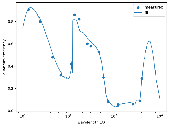
A model of the light-sensitive material of a Tektronix TK512CB sensor based on measurements by Stern et al. [1994].
This model uses
e2v_ccd64_thin()to represent the depletion region.Examples
Plot the measured TK512CB quantum efficiency vs the fitted quantum efficiency calculated using the method of Stern et al. [1994].
import matplotlib.pyplot as plt
import astropy.units as u
import astropy.visualization
import named_arrays as na
import optika

# Create a new instance of the e2v CCD97 light-sensitive material
material = optika.sensors.materials.tektronix_tk512cb()

# Store the wavelengths at which the QE was measured
wavelength_measured = material.eqe_measured.inputs

# Store the QE measurements
eqe_measured = material.eqe_measured.outputs

# Define a grid of wavelengths with which to evaluate the fitted QE
wavelength_fit = na.geomspace(10, 10000, axis="wavelength", num=1001) * u.AA

# Evaluate the fitted QE using the given wavelengths
eqe_fit = material.quantum_efficiency_effective(
    wavelength=wavelength_fit,
    direction=na.Cartesian3dVectorArray(0, 0, 1),
    normal=na.Cartesian3dVectorArray(0, 0, -1),
)

# Plot the measured QE vs the fitted QE
with astropy.visualization.quantity_support():
    fig, ax = plt.subplots(constrained_layout=True)
    na.plt.scatter(
        wavelength_measured,
        eqe_measured,
        label="measured",
    )
    na.plt.plot(
        wavelength_fit,
        eqe_fit,
        label="fit",
    )
    ax.set_xscale("log")
    ax.set_xlabel(f"wavelength ({wavelength_fit.unit:latex_inline})")
    ax.set_ylabel("quantum efficiency")
    ax.legend()
The thickness of the oxide layer found by the fit is
material.thickness_oxide
\[41.475836 \; \mathrm{\mathring{A}}\]The thickness of the implant layer found by the fit is
material.thickness_implant
\[2258.7289 \; \mathrm{\mathring{A}}\]The thickness of the substrate is
material.thickness_substrate
\[7 \; \mathrm{\mu m}\]The differential charge collection efficiency at the backsurface found by the fit is
material.cce_backsurface
\[0.1617392 \; \mathrm{}\]And the roughness of the substrate found by the fit is
material.roughness_substrate
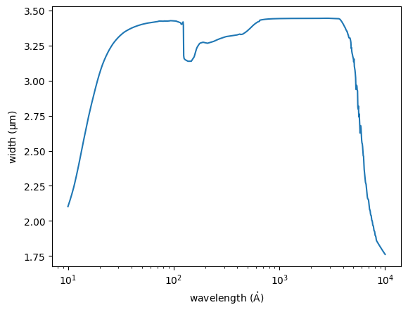
\[23.785294 \; \mathrm{nm}\]Plot the width of the charge diffusion kernel for this sensor as a function of wavelength.
# Compute the width of the charge diffusion kernel
# for each wavelength.
width = material.width_charge_diffusion(
    wavelength=wavelength_fit,
)

# Plot the results
with astropy.visualization.quantity_support():
    fig, ax = plt.subplots()
    na.plt.plot(
        wavelength_fit,
        width,
        ax=ax,
    )
    ax.set_xscale("log")
    ax.set_xlabel(f"wavelength ({ax.get_xlabel()})")
    ax.set_ylabel(f"width ({ax.get_ylabel()})")
References to
optika.sensors.materials.tektronix_tk512cb- Parameters:
temperature (Quantity | AbstractScalar)
- Return type: