charge_diffusion#
- optika.sensors.charge_diffusion(absorption, thickness_substrate, thickness_depletion)[source]#
The standard deviation of the charge diffusion in a backilluminated CCD given by Janesick [2001].
- Parameters:
absorption (Quantity | AbstractScalar) – The absorption coefficient of the light-sensitive layer for the incident photon.
thickness_substrate (Quantity | AbstractScalar) – The thickness of the light-sensitive region of the imaging sensor.
thickness_depletion (Quantity | AbstractScalar) – The thickness of the depletion region of the imaging sensor.
- Return type:
Examples
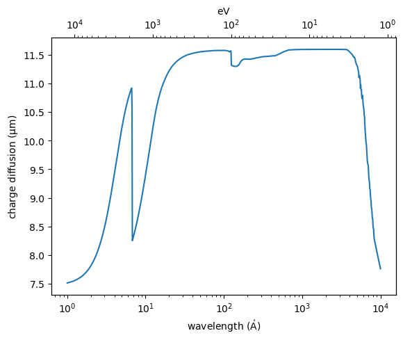
Plot the width of the charge diffusion kernel as a function of wavelength and energy for the sensor parameters in Heymes et al. [2020].
import matplotlib.pyplot as plt
import astropy.units as u
import astropy.visualization
import named_arrays as na
import optika

# Define a grid of wavelengths
wavelength = na.geomspace(1, 10000, axis="wavelength", num=1001) * u.AA

# Convert the grid to energies as well
energy = wavelength.to(u.eV, equivalencies=u.spectral())

# Load the optical properties of silicon
si = optika.chemicals.Chemical("Si")

# Retrieve the absorption coefficient of silicon
# for the given wavelengths.
absorption = si.absorption(wavelength)

# Compute the charge diffusion
width_diffusion = optika.sensors.charge_diffusion(
    absorption=absorption,
    thickness_substrate=14 * u.um,
    thickness_depletion=2.4 * u.um,
)

# Plot the charge diffusion as a function
# of wavelength and energy
with astropy.visualization.quantity_support():
    fig, ax = plt.subplots()
    ax2 = ax.twiny()
    ax2.invert_xaxis()
    na.plt.plot(
        wavelength,
        width_diffusion,
        ax=ax,
    )
    na.plt.plot(
        energy,
        width_diffusion,
        ax=ax2,
        linestyle="None",
    )
    ax.set_xscale("log")
    ax2.set_xscale("log")
    ax.set_xlabel(f"wavelength ({ax.get_xlabel()})")
    ax.set_ylabel(f"charge diffusion ({ax.get_ylabel()})")
Notes
The standard deviation of the charge diffusion kernel is given by Janesick [2001] as
\[\begin{split}\sigma_\text{cd}(x) = \begin{cases} x_{ff} \sqrt{1 - \frac{x}{x_{ff}}}, & 0 < x < x_{ff} \\ 0, & x_{ff} < x < x_s \end{cases}\end{split}\]where \(x\) is the distance from the back surface at which the photon is absorbed,
\[x_{ff} = x_s - x_d\]is the thickness of the field-free region of the sensor, \(x_s\) is the total thickness of the light-sensitive region, and \(x_d\) is the thickness of the depletion region.
The average variance of the charge diffusion kernel is then the weighted average,
\[\begin{split}\overline{\sigma}_\text{cd}^2 &= \dfrac{\displaystyle \int_0^{x_s} \left( \sigma_\text{cd}(x) \right)^2 e^{-\alpha x} dx} {\displaystyle \int_0^{x_s} e^{-\alpha x} dx} \\[1mm] &= \dfrac{\displaystyle \int_0^{x_{ff}} x_{ff}^2 \left( 1 - \frac{x}{x_{ff}} \right) e^{-\alpha x} dx} {\displaystyle \int_0^{x_s} e^{-\alpha x} dx} \\[1mm] &= \dfrac{x_{ff} \left( \alpha x_{ff} + e^{-\alpha x_{ff}} - 1 \right)} {\alpha \left( 1 - e^{-\alpha x_s} \right)}\end{split}\]where \(\alpha\) is the absorption coefficient of the light-sensitive layer.