electrons_measured#
- optika.sensors.electrons_measured(photons_absorbed, wavelength, absorption=None, thickness_implant=<Quantity 2317. Angstrom>, thickness_depletion=None, thickness_substrate=<Quantity 7. um>, width_pixel=<Quantity 27. um>, cce_backsurface=0.21, temperature=<Quantity 300. K>, axis_xy=None, wrap=False, shape_random=None)[source]#
A random sample from the distribution of measured electrons given the number of photons absorbed by the light-sensitive layer of the sensor.
This function accounts for both Fano noise and recombination noise due to partial-charge collection.
- Parameters:
photons_absorbed (Quantity | AbstractScalar) – The number of photons absorbed by the light-sensitive layer of the sensor.
wavelength (Quantity | ScalarArray) – The vacuum wavelength of the absorbed photons.
absorption (None | Quantity | AbstractScalar) – The absorption coefficient of silicon per unit perpendicular depth. For oblique incidence, supply the effective coefficient from
optika.sensors.absorption_effective(), which folds in the refracted angle, so no separate angle argument is needed.thickness_implant (Quantity | AbstractScalar) – The thickness of the implant layer, where partial-charge collection occurs.
thickness_depletion (None | Quantity | AbstractScalar) – The thickness of the depletion region, the region with significant electric field. If
None(the default), this is set to the same value as thickness_substrate.thickness_substrate (Quantity | AbstractScalar) – The thickness of the entire light-sensitive region of the device.
width_pixel (Quantity | AbstractScalar | AbstractCartesian2dVectorArray) – The size of a single pixel on the sensor. A scalar gives square pixels; a
named_arrays.AbstractCartesian2dVectorArraywhosex/ycomponents are the pixel widths alongaxis_xy[0]/axis_xy[1]gives rectangular pixels.cce_backsurface (Quantity | AbstractScalar) – The differential charge collection efficiency on the back surface of the sensor.
temperature (Quantity | ScalarArray) – The temperature of the silicon detector. Default is room temperature.
axis_xy (None | tuple[str, str]) – The two logical axes corresponding to the pixel grid of the sensor along which electrons will diffuse. If
None(the default), there is no charge diffusion.wrap (bool) – Controls how diffused charge is treated at the edges of the pixel grid. If
False(the default), charge that diffuses past the edge of the grid is lost, as it would be at the physical edge of a sensor. IfTrue, the grid is treated as periodic and the charge re-enters the opposite edge (a toroidal boundary).shape_random (None | dict[str, int]) – Additional shape used to specify the number of samples to draw.
- Return type:
Examples
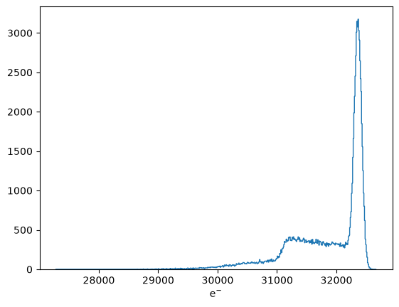
Plot the energy spectrum of twenty 6 keV photons emitted from an Fe-55 radioactive source.
import matplotlib.pyplot as plt
import astropy.units as u
import astropy.visualization
import named_arrays as na
import optika

# Define the number of experiments to perform
num_experiments = 100000

# Define the expected number of photons
# for each experiment
photons_absorbed = (20 * u.photon).astype(int)

# Define the wavelength at which to sample the distribution
wavelength = 5.9 * u.keV
wavelength = wavelength.to(u.AA, equivalencies=u.spectral())

# Compute the actual number of electrons measured for each experiment
electrons = optika.sensors.electrons_measured(
    photons_absorbed=photons_absorbed,
    wavelength=wavelength,
    shape_random=dict(experiment=num_experiments),
)

# Define the histogram bins
step = 10
bins = na.arange(
    electrons.value.min()-step/2,
    electrons.value.max()+step/2,
    step=step,
    axis="bin",
) * u.electron

# Compute a histogram of resulting energy spectrum
hist = na.histogram(
    electrons,
    bins=bins,
    axis="experiment",
)

# Plot the histogram
with astropy.visualization.quantity_support():
    fig, ax = plt.subplots()
    line = na.plt.stairs(
      hist.inputs,
      hist.outputs,
      ax=ax,
    )