charge_collection_efficiency#
- optika.sensors.charge_collection_efficiency(absorption, thickness_implant=<Quantity 2317. Angstrom>, cce_backsurface=0.21)[source]#
Compute the average charge collection efficiency using the differential charge collection efficiency profile described in Stern et al. [1994].
- Parameters:
absorption (Quantity | AbstractScalar) – The absorption coefficient of the light-sensitive material per unit perpendicular depth. For oblique incidence, supply the effective coefficient from
absorption_effective(), which folds in the refracted angle, so no separate angle argument is needed.thickness_implant (Quantity | AbstractScalar) – The thickness of the implant layer, the layer where recombination can occur. Default is the value given in Stern et al. [1994].
cce_backsurface (Quantity | AbstractScalar) – The differential charge collection efficiency on the back surface of the sensor. Default is the value given in Stern et al. [1994].
- Return type:
Examples
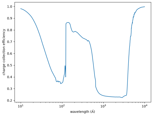
Plot the charge collection efficiency as a function of wavelength.
import matplotlib.pyplot as plt
import astropy.units as u
import named_arrays as na
import optika

# Define a grid of wavelengths
wavelength = na.geomspace(10, 10000, axis="wavelength", num=1001) * u.AA

# Compute the absorption coefficient for silicon
absorption = optika.chemicals.Chemical("Si").absorption(wavelength)

# Compute the CCE vs wavelength
cce = optika.sensors.charge_collection_efficiency(
    absorption=absorption,
)

# Plot the effective and maximum quantum efficiency
fig, ax = plt.subplots(constrained_layout=True)
na.plt.plot(
    wavelength,
    cce,
    ax=ax,
);
ax.set_xscale("log");
ax.set_xlabel(f"wavelength ({wavelength.unit:latex_inline})");
ax.set_ylabel("charge collection efficiency");
Notes
The charge collection efficiency is the fraction of photoelectrons that are measured by the sensor [Janesick, 2001], and is an important component of the quantum efficiency of the sensor
In Stern et al. [1994], the authors define a differential charge collection efficiency, \(\eta(z)\), which is the probability that a photoelectron resulting from a photon absorbed at a depth \(z\) will be measured by the sensor. In principle, \(\eta(z)\) depends on the exact implant profile on the backsurface of the sensor, however Stern et al. [1994] and Boerner et al. [2012] have shown that a piecewise-linear approximation of \(\eta(z)\),
(1)#\[\begin{split}\eta(z) = \begin{cases} \eta_0 + (1 - \eta_0) z / W, & 0 < z < W \\ 1, & W < z < D, \end{cases}\end{split}\]is sufficient, given the uncertainties in the optical constants involved.
The total charge collection efficiency is then the average value of \(\eta(z)\) weighted by the probability of absorbing a photon at a depth \(z\),
(2)#\[\text{CCE}(\lambda) = \frac{\int_0^\infty \eta(z) e^{-\alpha z} \, dz} {\int_0^\infty e^{-\alpha z} \, dz}.\]Plugging Equation (1) into Equation (2) and integrating yields
(3)#\[\text{CCE}(\lambda) = \eta_0 + \left( \frac{1 - \eta_0}{\alpha W} \right)(1 - e^{-\alpha W}).\]Equation (3) is equivalent to the term in curly braces of Equation 11 in Stern et al. [1994], with the addition of an \(e^{-\alpha W}\) term which represents photons absorbed inside the epitaxial layer but outside the implant layer.
In Equation (3), \(\alpha\) and \(z\) are measured along the surface normal. Oblique incidence is therefore handled entirely by the absorption coefficient: passing the perpendicular-depth coefficient \(\alpha_\perp\) from
absorption_effective()(which folds in the refracted angle, and reduces to \(\alpha\) at normal incidence) makes Equation (3) valid at any incidence angle without further modification.